Special Processes
Specialized PCB Processes
At United Electronic Corp., we excel in providing a comprehensive range of specialized PCB processes tailored to meet our clients’ diverse and demanding needs. Our commitment to innovation and quality ensures that we deliver exceptional products designed to support various high-performance applications.
Everyday Volume Capability
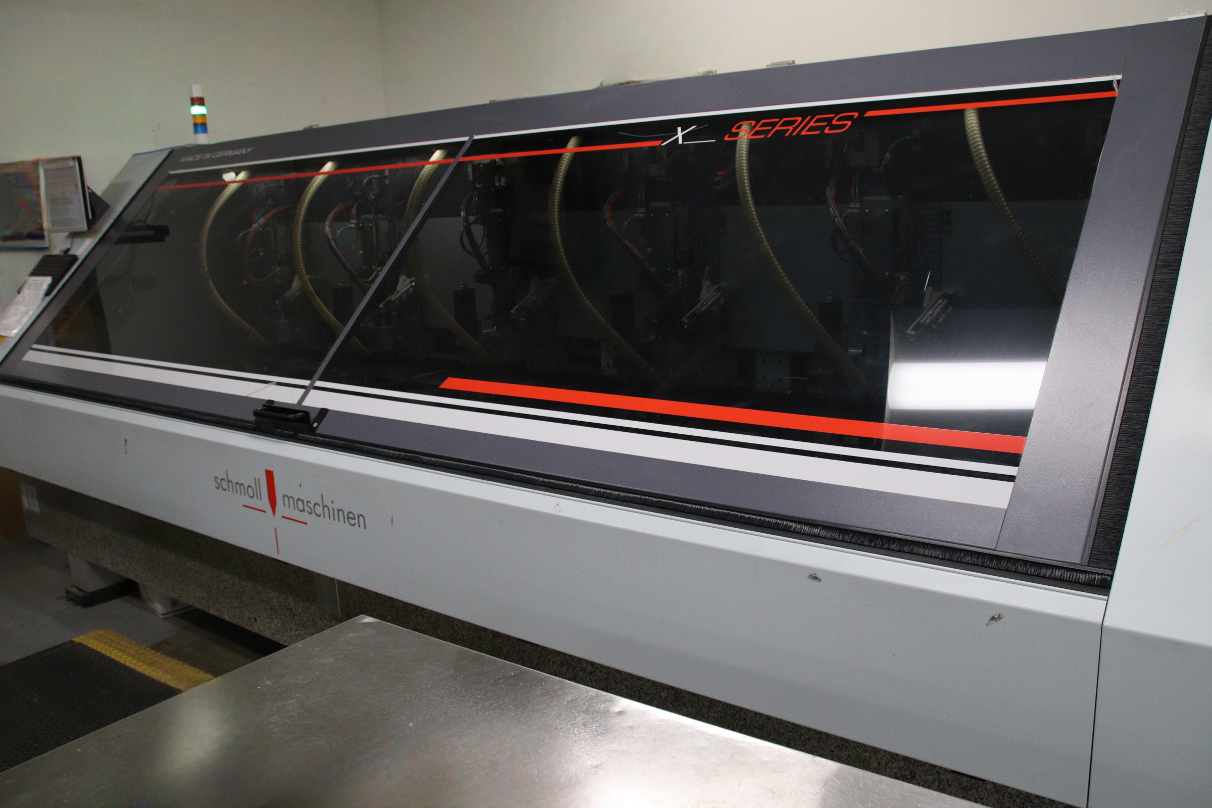
Our manufacturing capabilities cater to both small prototype batches and large-volume production, ensuring flexibility and scalability for any project. We can produce PCBs with up to 14 layers, featuring 3mil lines and spaces, panel thicknesses up to 250 mils, and controlled impedance within +/- 10%. Our specialized PCB processes include various types of final finishes, blind and buried vias, high-performance materials, sequential lamination, and both conductive and non-conductive via fill. Additionally, we support BGA and ultra-fine pitch designs, ensuring we meet the most intricate project requirements.
Advanced Materials
To meet specific application needs, we utilize a variety of advanced materials such as lead-free high Tg laminates (including Isola 370HR, Iteq 180, Ventec VT47), Teflon (Rogers, Taconic, Arlon, Nelco), standard FR4, polyimides, ceramics, and copper cladding with inner layer weights up to 4 oz and outer layers up to 8 oz.
Precision Etching and Drilling
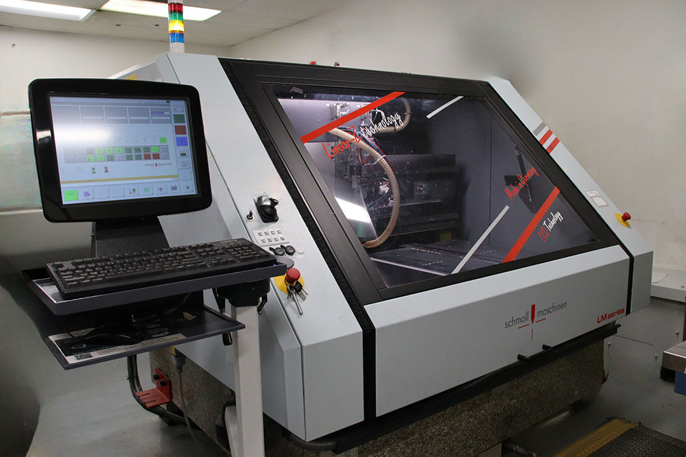
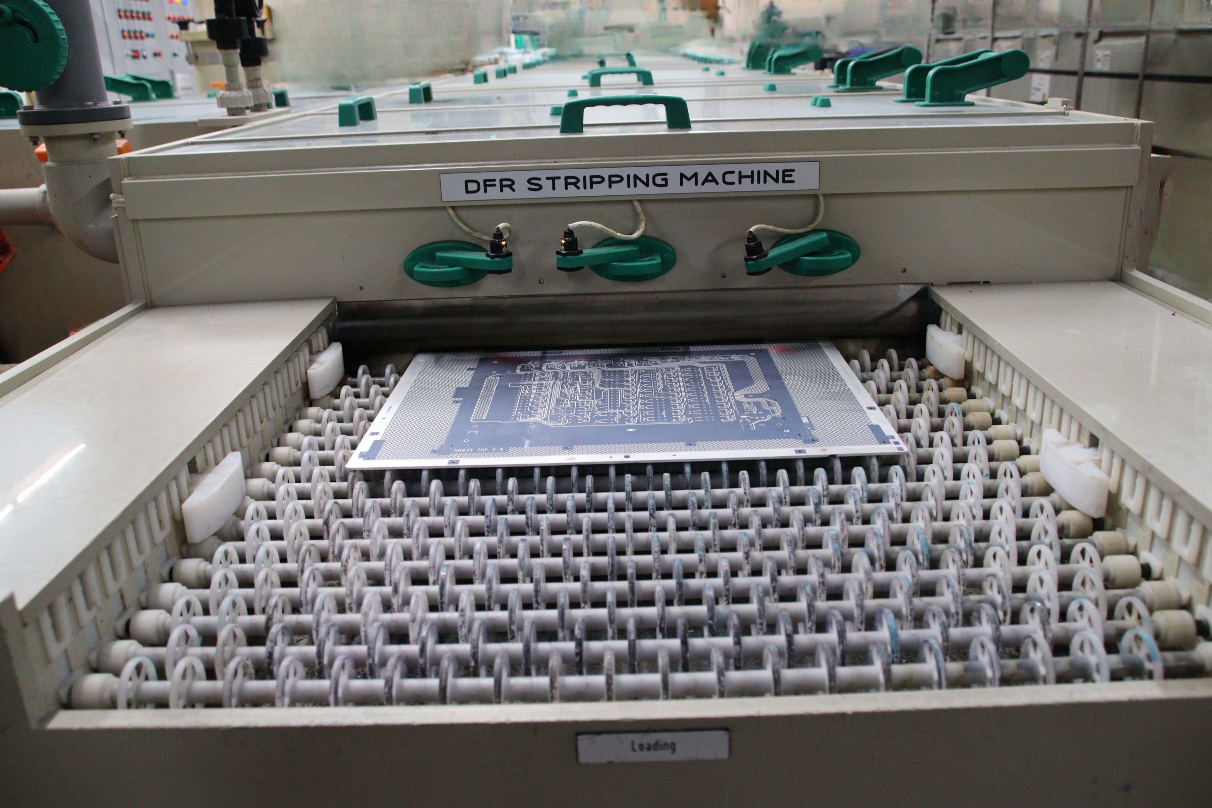
Our precision etching capabilities ensure fine detail and accuracy, with minimum conductor widths varying by copper weight, ranging from .003″ for 0.5 oz. foil to .007″ for 3.0+ oz. foil. We offer precise drilling and plating services, accommodating maximum aspect ratios of 10 to 1 and drilled hole sizes from 6 mil to 250 mil, ensuring high-quality standards with minimum annular plane clearances of .010″.
Comprehensive Finishes
United Electronic Corp. offers a comprehensive range of final finishes, including HASL (Hot Air Solder Level), lead-free HASL, ENIG (Electroless Nickel / Immersion Gold), electroless palladium, electrolytic hard and soft gold over electrolytic nickel, immersion tin, immersion silver, OSP (Organic Solderable Preservative), and carbon ink for switch pads. These finishes are integral to our specialized PCB processes and ensure compatibility with various applications and performance requirements.
Soldermask Processes
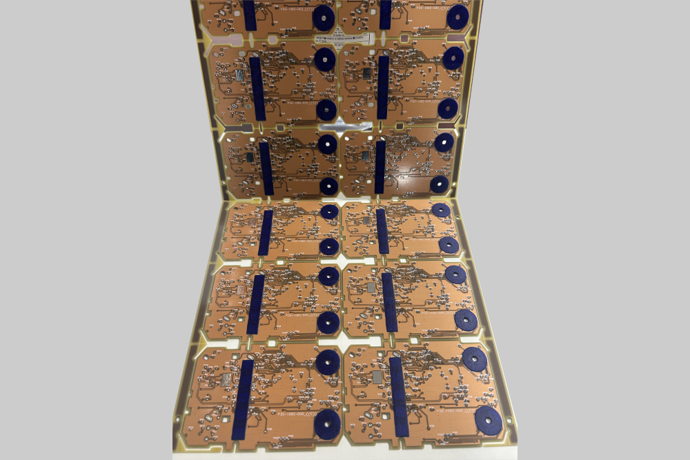
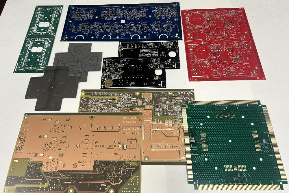
We employ various solder mask processes to meet specific needs, such as spray-coated photo-imageable solder masks, screened epoxy solder masks, screened UV-curable via plugging, and peelable masks with a stencil, with minimum solder mask clearances of .0025″.
Rigorous Electrical Testing
Our extensive electrical testing includes dual access testing, netlist testing, fixtureless testing, impedance testing with +/- 5% tolerance, minimum continuity tests of 10 Ohm, and maximum isolation tests of 10 M Ohm, ensuring the reliability and performance of our PCBs.
Precision Fabrication
Our precise fabrication services include scoring, web routing, edge milling, hard-tool pierce and/or blank, with minimum slot widths of .020″ and minimum distances of plated holes to internal traces of .0075″, ensuring the creation of complex PCB designs with high accuracy through our specialized PCB processes.
Via Fill and RF Telecommunication
We offer both conductive and non-conductive via fill solutions to enhance PCB performance and reliability. Our expertise in RF telecommunication includes complex board shapes, CNC routing and milling, machining tolerances down to ±.001″, and aluminum-backed PTFE circuits for heat management.

United Electronic Corp.’s specialized PCB processes allow us to handle power supplies, automotive electronics, computers, motor controls, and power semiconductors.
Ready to leverage our specialized PCB processes for your next project? Contact us to explore how our advanced capabilities can meet your specific needs and drive your success.
